Nintendo Entertainment System (NES) was created back in 1985 by the famous Japanese company Nintendo. It was an extremely revolutionary console at its time and was the best selling console for a number of years. I used to play NES a lot as a kid, so I have all those memories of the old games, and had an imminent urge to dig into the inner details of the console to figure out how it worked.

I got myself a Digilent Nexys 3 FPGA development board. It's a ready made FPGA board with built in Flash, RAM, USB programming interface, and power supply circuitry. This is a really quick and easy path into the world of FPGAs. The alternative could be to make the whole PCB from scratch, and that is something I want to learn some day. A guy named Kevtris has done exactly that with his FPGA Game Console.
There are two competing hardware description languages, VHDL and Verilog. I chose to learn Verilog because VHDL seemed unnecessarily verbose while Verilog offered a much more compact syntax.
The NES contains a Ricoh 2A03 CPU, virtually identical to the MOS 6502 CPU, but includes an on chip APU (Audio Processing Unit), while removing some CPU features such as Binary Coded Decimal arithmetic, supposedly to avoid paying patent royalties. Side by side to the CPU is a PPU (Picture Processing Unit), which is responsible for generating a 256x240 sized image. The console has extremely small amounts of memory with today's standards. It has a built in 2kB RAM for the CPU, and another 2kB used by the PPU. Additionally, some carts provided a few kilobytes of extra memory.
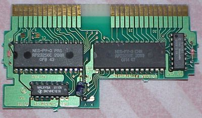 Since the CPU uses only a 16-bit address bus, it was common to include mapper chips inside of the cartridge. These are used to implement a mapping (or windowing) mechanism, so the CPU can select which part of the ROM to map into the address space. There exist a plethora of mapper configurations, around 200 different configurations or so. In some cases these were regular discrete logic chips such as 74LS161, while in other cases it was custom made ASICs. In order to support all NES games, I need to implement all those mapper chips too, as the FPGA NES uses an iNES ROM image instead of a physical cartridge.
The NES PPU runs off of a 21.4773 MHz crystal. This frequency was chosen by the original NES designers because it's the frequency used by NTSC video. These are the frequencies I make use of in my FPGA:
- 100MHz: The frequency of the devboard crystal, this gets converted down to 21.4773MHz by the FPGA's built in Digital Clock Manager (DCM) by first multiplying the frequency by 189, then dividing by 220, and finally dividing by 4.
- 21.4773MHz: The internal frequency the FPGA runs on, is used to clock the PSRAM logic, the VGA scanline doubler, ROM loader and some other top level logic.
- 5.37MHz: Generated by dividing 21.4773 by 4. This is frequency the PPU runs at, and every clock another pixel is outputted by the PPU. In my FPGA, I used clock enables to run the PPU only every 4th cycle, to avoid having multiple clock domains.
- 1.79MHz: PPU clock divided by 3. This clocks the CPU. Implemented as a clock enable that's active only every 12th cycle.
Here's a description of the various components that make up the FPGA NES:
Spartan 6 LX16 FPGA Core:
The heart of the board, the Spartan-6 is the programmable chip that runs the NES. It's a pretty advanced FPGA where the basic building block is a 6 input LUT instead of the more commonly used 4-input LUT used in the Spartan-3 series. Here's an FPGA Logic Cells comparison with more info.
The LUT is used to create an arbitrary function of 6 bits of inputs into one bit of output, i.e. 2^6=64 bits of state. These LUTs get interconnected and state is persisted between clock cycles through the use of flip flops, which each keep 1 bit of memory.
16Mbyte Micron Cellular RAM
This is PSRAM, a hybrid of a cheap DRAM and a more expensive SRAM. It still requires DRAM refresh cycles, but all that is happens behind the scenes so I don't need to worry about it. The RAM has an access time of 70ns, meaning that after I put the address out on the bus, I need to wait 70ns before the data is available for me to read. In my RAM logic, I wait 2 cycles (90ns). I timed it so I perform one single byte fetch per PPU clock.
The NES has separate address buses for the CPU (code) and the PPU (graphics). Since I use a single RAM chip, I'm time multiplexing the accesses. The PPU accesses ram only every second clock cycle, i.e. 50% of the time, while CPU accesses every third PPU cycle (33% of the time).
8-bit VGA
 This is a rather mediocre video solution, as it only gives me 3 bits for Red, 3 bits for Green and 2 bits for Blue. This only allows for 4 levels of grayscale, so I can't even represent all NES colors accurately (see the picture). I need to move away from this once I figure out a better solution. I really wish the Digilent board would have used a proper video DAC instead, such as Analog Devices ADV7123.
PMOD Connector
 These are Digilent's own expansion connectors. I created some simple audio circuitry using a 16 bit AD1866 Audio DAC connected to a single supply Operational Amplifier. The Audio DAC has a bit limited voltage range, 1.5V - 3.5V, so the peak to peak voltage after the opamp is only around 1 volt or so. I discovered the hard way by trial and error that I had to connect an electrolytic capacitor in series with the speaker to act as a high pass filter and remove the DC component to get the average voltage down to 0 volts instead of 2.5 volts.
USB Interface
The Digilent USB Interface can also be used as a bidirectional communications channel between the FPGA and a program running on the PC. The only controllers I had were USB SNES controllers, so I hooked the controller up to the PC and have a small program that reads the joystick movements and sends these over the cable to the FPGA.
6502 CPU Core
I wrote my own 6502 Verilog core, it seemed like a fun challenge and was a lot more educational and challenging than just stealing someone else's. The CPU contains an ALU, a set of registers, and a datapath structure that connects these together. Each instruction runs in a variable number of cycles, and a big microcode table controls which muxes and control signals that are active for every cycle of an instruction. There exists a lot of good documentation of how the 6502 worked down to the cycle level.
Interestingly, the 6502 had a bunch of undocumented instructions. These exist because instructions are only partially decoded by a Decode PLA, and the unused opcodes trigger random control signals in the CPU, causing unplanned things to happen. I implemented most of these, except for some very esoteric ones.
APU (Audio Processing Unit)
The NES APU contains 5 tone generators: Two square wave generators, one triangle generator, one noise generator and a DMC (Delta Modulation Channel). These are periodically controlled by the CPU by writing to a few IO registers in the APU. The outputs of these 5 channels are then combined in a way to mimic the audio hardware of the NES, by using a few look up tables implemented on the FPGA's block ram.
Because the sample frequency of the APU is 1.79MHz, and the output frequency of my DAC is much much lower, I need to implement a digital low pass filter to remove the very high frequency components, to avoid aliasing artifacts. I implemented a 767 order FIR filter using one of the FPGA's DSP Multiply and Accumulate units and some block ram. The DSP unit can compute expressions on the form P = P + A * (B + C) in a single clock cycle. The FIR filter runs at 21.4773 MHz, and generates an output sample rate of 1/384th of that (55.9 kHz). Thanks to FIR filters being symmetrical, I only need to perform 768/2 = 384 multiplications per output sample, i.e. exactly one multiplication per clock cycle.
PPU (Picture Processing Unit)
Generates output pixels and VGA control signals so the picture can be output on a standard PC monitor. I use the output resolution 512x480, so I implemented a scanline doubler in the FPGA, so that one PPU pixel becomes a 2x2 pixel on the VGA screen. The PPU implements the NES tile engine, where the screen is made up of a 32x30 8x8 pixel tiles, and there can be 64 sprites each either 8x8 or 8x16 pixels. The PPU aims to be completely cycle accurate, or else there will be glitches in certain games that depend on the exact NES clock timing.
Mappers
So far I've only implemented a subset of all mappers that exist.
MMC1: Nintendo ASIC, used in Megaman 2, Zelda, Metroid.
MMC2: Nintendo ASIC. The only game that uses this seems to be Punch Out. It contains some dynamic bank switching to allow for more tiles than normal to be displayed on the screen simultaneously.
MMC3: Nintendo ASIC, used in Megaman 3,4,5, Super Mario Bros 2,3. This mapper features a pretty interesting scanline counter that counts the number of transitions on the address lines. By making some assumptions on the pattern at which the PPU accesses things, an IRQ can be generated to the CPU when a certain scanline is about to be rendered. This is mostly used for split screen effects.
Tepples Multi Discrete Mapper: A single mapper that can be reconfigured to support several different discrete logic mappers. I reuse this code path to implement support for the UxROM, CNROM, AxROM mappers.
Results
Here is a photo of the result:

Spartan 6 LX16 Utilization:

Gratulations!
ReplyDeleteThis is so nice man.
What I can say...
Good Job, RESPECT!
People like you can change the world...
Can u build an Atari for me? :-)
Cheers
L@usch
@L@usch
ReplyDeleteBuild an Atari (2600) for you? Been done...
http://hackaday.com/2010/09/15/atari-2600-recreated-in-an-fpga/
Or perhaps you meant an Atari (ST)? Been done as well...
http://experiment-s.de/en/
@Ludde
Great work. :-)
This is awesome! I remember taking an FPGA class in college. We used VHDL, and I agree it is very verbose. Nice job.
ReplyDeleteawesome! Hope you get bored more often :)
ReplyDeleteOut of curiosity - how long did it take to develop, from empty project to the working prototype?
ReplyDeleteI'm curious to know the same thing
DeleteGreat work!
ReplyDeleteIs it possible to download Verilog code and schematics?
Awesome project. Would love to see this open-sourced.
ReplyDeletetime needed from the start of the project to the end ? (weeks,months)
ReplyDeletethanks
I spent about a 4-5 weeks on the project
ReplyDeleteHello there,
ReplyDeleteI'm curious about how the PPU inside actually work. Do you have a block diagram or a simple flowchart on how it all works? I've read the PPU documentation online but not much on the image generation mechanism is explained inside.
Thanks,
B.
The PPU portion of this design could be used to make a drop-in PPU replacement for the NES itself, allowing for true RGB (or component) output from the NES without having to source a PPU from a playchoice 10.
ReplyDeleteHey Ludde,
ReplyDeleteI'm just getting started in Verilog. Can you recommend any books or tutorials you used to get up to speed?
Thanks.
Hi, I have made an HDMI interface for the Nexys 3 if you are interested, it use the VHDCI connector and a VMOD MIB from digilent. You can display up to 1080i resolutions
ReplyDeleteAlso i have an Hq2X scaler implemented in the nexys3
DeleteThat sounds nice. How much resources does it use?
DeletePossibly I'm not as helped by Hq2X as long as I use a 8bit VGA..
The HQ2X module is not in my computer so I Can't check right now. But the HDMI, uses very few resources. It use 215 slice registers and 85 LUT, 2 BRAMS, and one PLL.
DeleteThe HQ2X use more resources, it use at least 3 dedicated multipliers, because a online transformation from RGB to YUV was neddeed.
DeleteIf you wanna contact me for any assistance I'll be happy to provide it. Your proyect is a quite interesting one.
I already made my own HQ2X, see the blog post :)
DeleteNice implementation, mine is not an aproximation but uses a lot more resources than yours.
DeleteWhat about the HDMI, you could use an HQ3X and made an output a 720p (with black bars at the sides)
Hi Alejandro,
Deleteis your code available somewhere? I recently tried to port some code from Xilinx of an AppNote to exactly this Nexys 3 + VmodMIB combination, but I always failed because of some routing issues I still couldn't figure out. That would be awesome!
No, It is not available, but as long as you don't publish it as if it was yours. I could send it to you
DeleteNevermind, I got it to work by myself: https://github.com/G33KatWork/nexys3_hdmi
DeleteThanks anyway!
Hi. This project is awesome! Really nicely done! I am also creating a NES on FPGA for my engineering degree. Can you contact me if i would need any help so i can ask you for assistance, and also can You say from where you got the RP2C02 datasheet or information how to write it(how it is built?).
ReplyDeleteWould it be possible to use with NES cartridges ?
ReplyDeleteCongratulations to a great project. Also a good and interesting write-up of what you've done.
ReplyDeleteI've also been fiddling around FPGA's for some years. They're great fun! Visit my page at: http://www.wedmark.se. For now just a small project to emulate the tv-test picture.
Now I understand the PSRAM that I've read about earlier. I really like a slower/bigger SRAM but you can skip the logic handling the banking, refresh and stuff. But does it remove the possibility to do fast bursts?
You should really release the source code for other to look at, learn from and add stuff. GoogleCode is great where you can keep control of it and add the stuff you like and tested yourself.
I have a simple/hack suggestion for your missing color. Just create a maximum clocked pixel-clock that switches between colors internally for each pixel. I think this works best for old analog CRT-VGA screens and maybe introduce problems to some TFT-monitors using digital filter.. Anyway, this way you can use the existing hardware, but still show some more colors. I've tried this some years ago with my Xilinx Spartan-3 Starter kit and its 3-bit color (only 1-bit per R,G,B) with quite good result. Using a overclocked 280Mhz FreqMax color-clock on my 25Mhz original pixel-clock (640*480@60Hz) I've got an effective X-resolution of about 7040 usable pixels per line, but still keeping the V-sync/H-sync timing so the monitors think it's just the normal 640*480 resolution. The VGA-lead and connectors filter out the highest frequencies actually helping out with blending the colors. The result in my case was that I could extend each color (R,G,B) from 1-bit (0-1) up to about 3/4-bit (0-11) and at least have 512 colors.
In your case maybe extending the missing bit on Blue would be enough, using just one dithered pattern of f.e. 1010'1010 running @200Mhz. => 3-bit Blue!
Another way would be to create the NTSC/PAL signal yourself. This would of course make it look even more like the real-deal.
Good luck in future FPGA-hacking.
Best Regards
Magnus
I would love to see that code... I am working on the same sort of thing, but I cannot get timing to be as good as I want it to be.
ReplyDeleteCould I please have a look at your code (I am asking if you could send it to me)
Great job! thanks for share it! Could I use a spartan 3E to implement it? I got Nexys 2 board
ReplyDeleteThank you very much.
Hi, can we use your NES FPGA development in our open source project ZXUno?
ReplyDeletehttp://www.aiobjectives.com/2019/12/18/what-is-forgery-why-it-is-fraud/
ReplyDeleteWhat is forgery crimes and why it is fraud ?. Forgery crimes is fake signature and without
permission making a false documents or every where.
What is duplicate invoices and waht is processed of duplicate invoices and what
is detict of this crimres.
islamic dua fuaktsoft channel is the best channel to promote our children to religon and prompte the attention levelof our children.
ReplyDeleteIn Islam, Invocation (duʿāʾ) (Arabic: دُعَاء IPA: [duˈʕæːʔ], plural: ʾadʿiyah أدْعِيَة [ʔædˈʕijæ]) is a prayer of
supplication or request. ... Muhammad is reported to have said, "Dua is the very essence of worship."
Poetry has so many benefits for kids. It is not only a great medium for rendering information
ReplyDeletebut children also find poems very delightful. Poetry recitation and memorising is a fun activity that you can
engage your kid in. Let’s take a look at some famous, funny and rhyming poems for kids. Along with that, we shall
discuss how you can select a poem and teach your kid to recite it.
https://www.youtube.com/watch?v=pQ7_elTLT2k&list=PLGdtwx2xwTkV0MYq8uC1BBUUpRwJwJ98Q&index=2
ReplyDeleteOur main goal is to train and educate our kids or children through different Rhymes for kids and attractive poems for children
sugar daddy sayesinde hayalinizdeki zengin ve lüks hayata hemen sahip olabilirsiniz.
ReplyDeleteinstagram beğeni satın al aradığınız tüm sosyal medya hizmetleri bir yerde
ReplyDelete
ReplyDeletebarbaroslar episode 1 in urdu
Comment for barbaroslar episodes: Go and Watch the Turkish Drama Series of Engin Altan's "Barbarosslar" in Urdu only on our youtube channel "My Kids Tube".
Please subscribe and Stay Tuned!
https://www.youtube.com/watch?v=qmJQOLaK2IM
very good article thnx for sharing good information i really appriciete . i read blog on daily.
ReplyDeleteTitle Town Advisers mission is to work with small to large business owners to achieve their goals,
assist with business development, and reach the audience they desire. In addition,
we stride to provide quality and effective services to our clients. Finally,
TTA’s desire is to create economic stimulus and freedom to our clients.